
Research
Contents

1. Introduction
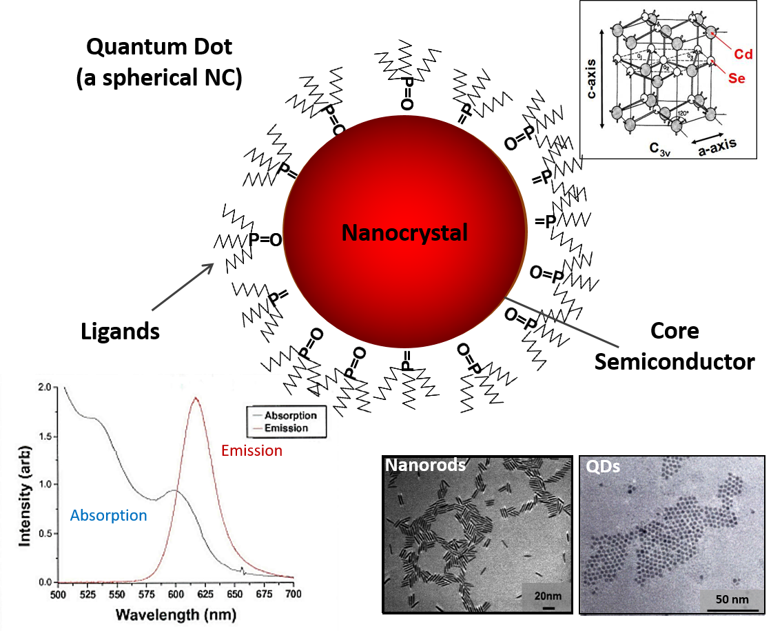
Colloidal semiconductor nanocrystals, including quantum dots, nanorods, tetrapods, 2-D materials and other low dimensional structures are of great interest for a variety of applications. In our group we use colloidal chemical synthesis techniques to produce novel nanomaterials with applications in LEDs, solar cells, photodetectors and other optical and electronic device applications. Nanocrystals produced using these methods consist of a core of a single crystalline material, or a core-shell, doped or graded crystal structure, surrounded by a ligand shell. The outward facing functional groups of the ligands can be changed to change the dispersibility of the NCs and allow the NC to be attached chemically to other molecules, NCs or surfaces.
Probably the most important characteristic of these nanocrystals is the tunable bandgap, which distinguishes nanocrystals from larger crystalline compounds. Here the band edge of the NC can be tuned by size, composition (including core-shell, grading or alloyed materials), crystal structure or by doping the crystalline material. It is this broad strong absorption and thin tunable emission linewidth of the NCs that make them such promising materials for optoelectronic
applications. In addition, by changing the ligand groups and synthesis methods, we can control the conduction properties of the NCs by changing the density and energy level of charge traps on their surfaces. This gives us a large number of interesting physical effects by which we can use these materials for charge transport, light harvesting, charge storage, and other electronic properties.
Metal halide perovskites nanostructures have recently gained interest as a new class of earth-abundant semiconductor materials that are suitable for many optoelectronic applications including in light-emitting diodes (LED), lasers, and (X-ray) photodetectors. Although we work on a range of material sets, our group is currently focused on inorganic perovskite nanocrystals as a great material for optoelectronic applications.
2. Nanocrystal Synthesis
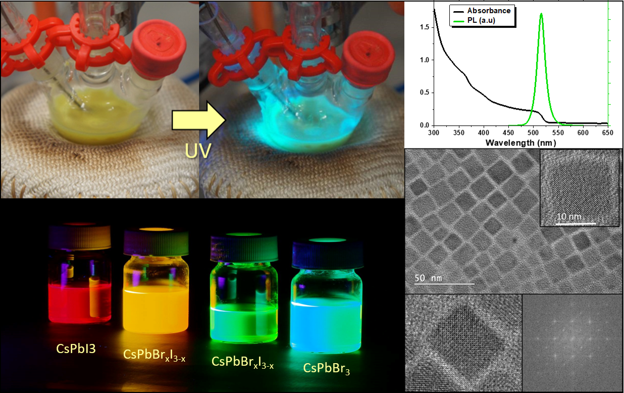
Inorganic perovskite quantum dots tend to have higher stability and better photoelectric performance than organic/inorganic hybrid perovskites. A typical synthesis of perovskite nanocrystals includes the following steps:
- Synthesis of halide and metal precursor materials
- Degassing of surfactants and precursors
- Hot injection of metal precursor at varying reaction temperatures
- Cooling of the reaction medium upon achieving the desired size, shape and size distribution
- Solvent/anti-solvent purification
These perovskite quantum dots and 2-D materials exhibit compositional-tunability through the entire visible spectral
region of 420–700 nm. Some halide quantum dots are able to show surface passivation effects and these can be used to reduce the presence of non-radiative traps. By varying the concentrations of the reagents, the time of the reaction, the ligand concentrations and the temperatures of injection and reaction, we can tune the properties of these materials to create a range of sizes and shapes.
3. Light Emitting Devices (LEDs)
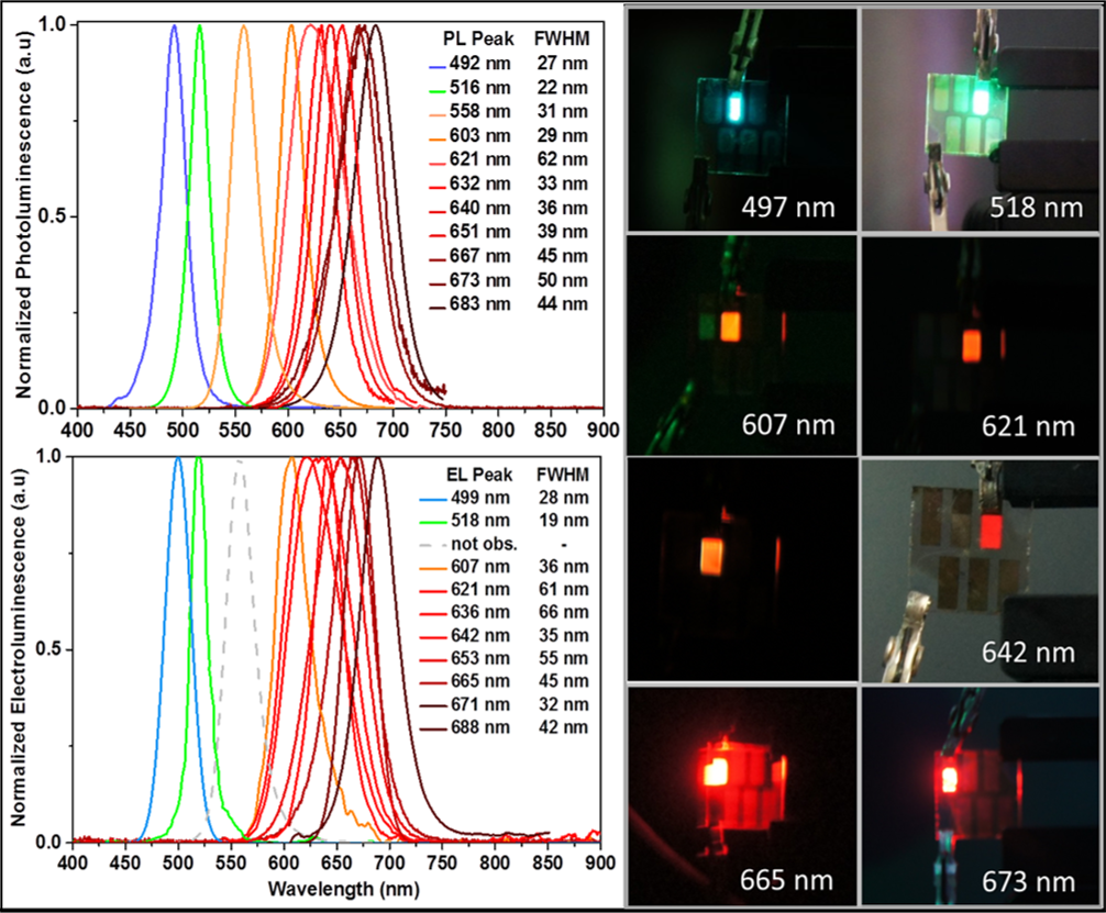
The greatest strength of QDs for light-emitting applications is their tunable bandgap and high quantum yield. It is for these reasons that perovskite nanocrystals are interesting for nanocrystal light-emitting devices (LEDs).
In a basic QD light-emitting diode device structure, the QD layer is sandwiched between an electron-injecting cathode and a hole-injecting anode. Under an applied field, carriers injected from the cathode and anode and recombine in the perovskite nanocrystal emissive layer. The active layer emits visible light when holes and electrons radiatively recombine within them. Quantum dot LEDs use semiconductor nanocrystals as the active layer instead of a thin film of molecules or a crystalline thin film.
We have recently synthesized mixed halide CsPbBr3-xXx (where X = I, Br, Cl) perovskite nanocrystals with photoluminescence across the visible region to produce LEDs displaying EL across the visible spectrum [1]. In low dimensional perovskite nanocrystals, carriers may combine to form relatively long lived excitonic states, while in larger bulk-like NCs, screening from the surrounding medium produces mainly free charge carriers that recombine via band-to-band recombination.
Our work in this field includes improving the efficiency, longevity and emission stability of these devices. Although QD-LEDs have been around for a while, there is still a great deal of interest in finding new materials with superior electronic and emission properties, especially if these can be produced without using toxic metals.
4. Solar Cells

Metal halide perovskites are one of the most popular new materials in photovoltaics (PV) research today. Recently perovskite semiconductor materials have shown significant potential in photovoltaics because of their high power conversion efficiency (PCE > 22%) and their low cost of fabrication. There are currently three main perovskite compounds suitable for photovoltaics applications: MAPbX3, FAPbX3 and CsPbX3 (where X=Br/I or I/Cl).
The general architecture of perovskite solar cells can be either p-i-n or n-i-p structure, where the perovskite is an intrinsic semiconductor, and light enters through the n–type or the p-type layer, respectively. The structure consists of mainly three functional layers: the electron transport layer (ETL), the light absorber layer (perovskite) and the hole transport layer (HTL). The figure here shows a schematic representation of an example of the most common (early) device type, which ressembles a titania dye sensitized solar cell (DSSC).
We have recently introduced a dynamically dispensed
spin-coating technique that uses a two-step deposition method to form a perovskite layer with an arbitrarily controllable quantity of crystalline PbI2 [2]. We have introduced nanocrystals into the perovskite solar cell, in the form of copper indium sulfide nanocrystals (CIS NCs), to aid in light absorption, as a charge transport/charge blocking layer, and to improve water resistance. We were able to achieve enhanced charge transfer property as well as longer lived films and devices [3].Figure shows some of our earlier perovskite devices. Our current research on perovskite involves the following features. 1. for solution processed perovskite devices, improving the device engineering and modification of charge-transport behavior at interfaces 2. Improving stability and lifetime of the devices by by using inorganic nanocrystals. 3. We are also looking at the fundamental materials and device physics using various spectroscopy techniques, charge transfer studies and our future work includes theoretical modelling to attain the highest efficiency of the devices.
5. Physics & Spectroscopy
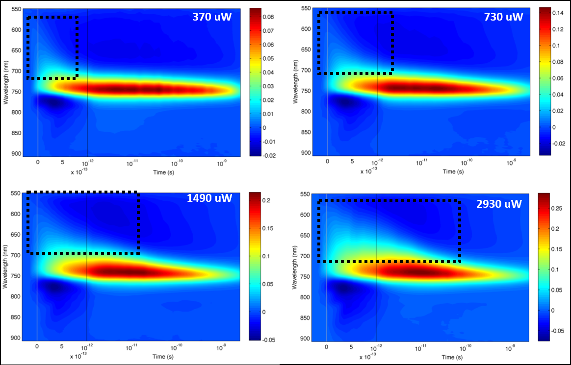
Optical spectroscopy is a fundamental tool for understanding the photophysics of nanocrystals. We have been collaborating with several research groups to study the fundamental physical properties of metal halide perovskites. Our collaboration work, particularly with the Hodgkiss group at VUW, includes transient absorption (TA) spectroscopy analysis, ultrafast broadband photoluminescence studies, and analysis of charge transfer dynamics. This work allows us to characterize our nanomaterials and also to make significant contributions to the understanding of photophysics for our novel materials.
Recently we have studied TA spectral dynamics of CH3NH3PbI3–xClx and carried out research on carrier thermalization dynamics [5] . Subsequently, we have also studied the ultrafast transient absorption study of cubic CsPbBr3 NCs as a function of size, as compared with the bulk material and larger NCs [6].
We are also involved in collaborations with theoretical groups, modelling the optical and electronic properties of quantum dots and clusters, using VASP. These studies are expected to be published soon.